2026年10月13日
材料,DIS/設計,アドボカシー&ポリシー,半導体製造装置メーカー
Japan–U.S. Semiconductor Collaboration Forum 2026
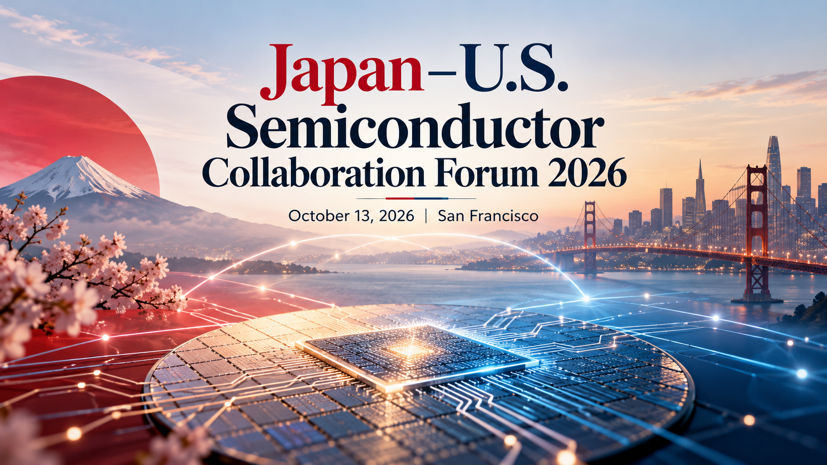
The forum will bring together semiconductor companies, startups, policymakers, and ecosystem partners from Japan and the United States to explore opportunities for practical business collaboration. The program will highlight the complementary strengths of the two semiconductor ecosystems, including U.S. capabilities in semiconductor design and fabless innovation and Japanese strengths in materials, equipment, advanced packaging, and manufacturing. The forum is designed to go beyond policy discussions and create opportunities for companies to identify potential partners and explore concrete areas for future collaboration.
<本フォーラムについて>
本フォーラムでは、日本と米国の半導体企業、スタートアップ、政策関係者、エコシステムパートナーが一堂に会し、具体的なビジネス連携の可能性を探ります。プログラムでは、半導体設計やファブレス分野に強みを持つ米国と、材料・製造装置・先端パッケージング・製造分野に強みを持つ日本、それぞれの半導体エコシステムの特徴や相互補完性に焦点を当てます。政策面での議論にとどまらず、参加企業同士が新たなパートナー候補と出会い、今後の具体的な協業テーマやビジネス機会を検討するきっかけとなることを目指しています。
- 日時
- October 13, 2026 (Tue), 4:00–6:30 PM (PDT)
※ Japan Time: October 14, 2026 (Wed), 8:00–10:30 AM
- 場所
- San Francisco, United States(Venue details will be shared after registration)
- 参加対象者
- The event is intended for companies and organizations across the semiconductor ecosystem, including:
・Semiconductor design and fabless companies
・Semiconductor startups
・Materials and equipment companies
・Advanced packaging and manufacturing companies
・Investors, accelerators, and ecosystem builders
・Companies interested in Japan–U.S. business collaboration
- 費用
- Free
- 申込締切
- October 7, 11:59 PM (GMT-7)
- 募集期間
- - 〜 -
- 定員
- お問合せ先
- Please contact the organizer via “Contact the Host” on the Luma event page.
- 主催
- Co-hosted by: Japan External Trade Organization (JETRO) San Francisco, California Governor’s Office of Business and Economic Development (GO-Biz)
Supporting Organization: Consulate-General of Japan in San Francisco, NEDO Silicon Valley, Japanese Chamber of Commerce of Northern California (JCCNC), Japan Society of Northern California (JSNC), RISE-A, Japan Materials Network, Silicon Valley(素材の会), CHIP-J.org(シリコンバレー半導体勉強会)
- 備考/注意事項
- This is a complimentary event, and participation is subject to approval. Only participants whose registrations have been approved will be able to attend the Forum. Walk-ins will not be permitted.
Click to Register;https://luma.com/00akbxdy
タイムテーブル
登壇者プロフィール
Program
| 時間 | 内容 |
| 4:00 PM | Open Door |
| 4:30 PM | Opening Remarks Remarks from representatives of JETRO, the Consulate-General of Japan in San Francisco, and California Governor’s Office of Business and Economic Development (GO-Biz) |
| 4:40 PM | Keynote Speeches Topics are tentative and subject to change. California GO-Biz: California’s semiconductor policy and industry ecosystem Japan’s Ministry of Economy, Trade and Industry (METI): Japan’s semiconductor policy and recent industry developments |
| 5:00 PM | Panel Discussion Opportunities for Japan–U.S. Collaboration in the Semiconductor Sector Moderator: Paul Pickering, Managing Partner, Silicon Catalyst Panelists: To be announced |
| 5:20 PM | Pitch Session Reverse pitches by Japanese companies presenting their collaboration needs and partnership interests Pitches by U.S. and California startups and companies seeking collaboration with Japanese partners |
| 5:45 PM | Networking *Additional speakers and participating companies will be announced soon. |
| 6:30 PM | Door Close |


